CSR Unit (Control and Status Register)
Overview
The CSR Unit provides the structural storage and bitwise manipulation logic required to support the RISC-V Zicsr standard extension alongside dedicated custom testing registers. It handles state tracking for status, control, performance metrics, and hardware diagnostic environments.
- Purpose in CPU: Executes atomic read-and-modify operations on Control and Status Registers (CSRs), enabling software-level system management, trap/interrupt configuration, OS context switching, and testbench evaluation.
-
Role in datapath: Positioned in the Memory (MEM) stage of the pipeline. It reads the current register state to supply the Writeback (WB) path for the general-purpose register file (
rd) before executing the requested bitwise modifications via an internal transformation matrix and writing the updated value back to the discrete register elements. -
Source:
logisim/RiskVMemory.circ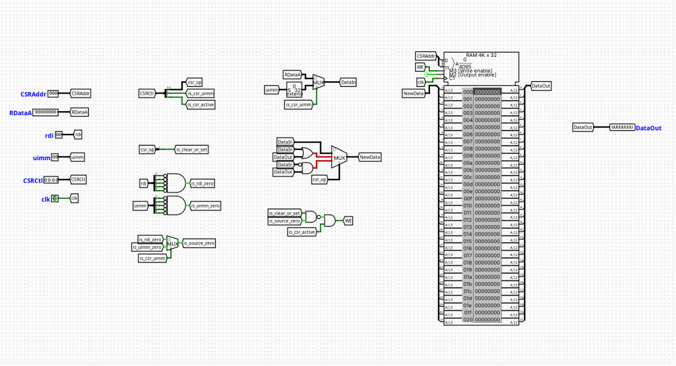
Interface
Inputs
| Signal | Width | Description |
|---|---|---|
CSRAddr |
12 | The 12-bit absolute address specifying which CSR register to access (from the instruction payload). |
RDataA |
32 | The forwarded data value read from general-purpose register rs1, used as the operand for register-source variants. |
rdi |
5 | The raw 5-bit register source index from the instruction (instruction[19:15]), used for register-zero detection. |
uimm |
5 | The raw 5-bit immediate value payload from the instruction (instruction[19:15]), used for immediate-zero detection. |
CSRCtl |
4 | Packed unified control bus: CSRCtl[3] = Active flag, CSRCtl[2] = Source selection, CSRCtl[1:0] = Bitwise operation code. |
is_valid_inst |
1 | Pipeline validity bit tracking from the Writeback (WB) stage; asserts high when a non-bubbled instruction successfully retires. |
clk |
1 | Master system clock signal driving the synchronous write operations of the internal storage block. |
Outputs
| Signal | Width | Description |
|---|---|---|
DataOut |
32 | The old read data extracted from the CSR memory block prior to modification, routed to the WB stage multiplexer. |
Output Logic (Core Definition)
Rule-based definition
- Master Execution Validation:
is_csr_active=CSRCtl[3]is_csr_uimm=CSRCtl[2]-
csr_op=CSRCtl[1:0] -
Zero-Operand Suppression Loop:
- If
rdi == 5'b00000→is_rdi_zero = 1 - If
uimm == 5'b00000→is_uimm_zero = 1 -
is_source_zero=is_csr_uimm?is_uimm_zero:is_rdi_zero -
Modifier Instruction Extraction:
-
is_clear_or_set=csr_op[1] -
Write Enable Generation (
WE): - If
is_csr_active == 1and(is_clear_or_set NAND is_source_zero) == 1→WE = 1 -
Otherwise →
WE = 0 -
Internal Data Modification (
NewData): - If
csr_op == 2'b01(Write) →NewData = DataIn - If
csr_op == 2'b10(Set) →NewData = DataOut OR DataIn - If
csr_op == 2'b11(Clear) →NewData = DataOut AND (NOT DataIn)
Boolean expressions
is_clear_or_set = CSRCtl[1]
is_source_zero  = (CSRCtl[2]) ? is_uimm_zero : is_rdi_zero

WE = CSRCtl[3] AND (is_clear_or_set NAND is_source_zero)
Register Map & Address Decoding
The component implements discrete 32-bit registers configured with dedicated address decoding logic flags rather than a continuous RAM block.
1. Performance Counters (Continuous Hardware Accumulators)
These units utilize an internal feedback adder loop. Their local register write enables (EN) are hardwired constantly high (1), meaning they update synchronously every clock cycle.
| Name | Address (Hex) | Access Type | Structural Behavior |
|---|---|---|---|
cycle |
12'hC00 / 12'h300 |
Read-Write | Automatically increments by 1 every clock cycle via an adder feedback loop unless overwritten by software NewData. |
instret |
12'hC02 / 12'h302 |
Read-Write | Automatically increments by 1 via an adder feedback loop whenever is_valid_inst == 1 at the clock edge unless overwritten by software NewData. |
2. Machine & Supervisor Control Registers (Privilege Infrastructure)
These units hold operating system and trap-handling states. They only commit updates when explicitly written by software operations matching their address, or via hardware trap controllers.
| Name | Address (Hex) | Access Type | Description |
|---|---|---|---|
mstatus |
12'h300 |
Read-Write | Machine Status: Tracks global interrupt states and privilege levels. |
medeleg |
12'h302 |
Read-Write | Machine Exception Delegation: Routes exceptions directly to S-mode. |
mideleg |
12'h303 |
Read-Write | Machine Interrupt Delegation: Routes interrupts directly to S-mode. |
mtvec |
12'h305 |
Read-Write | Machine Trap-Vector Base-Address: Base address for M-mode handlers. |
mepc |
12'h341 |
Read-Write | Machine Exception Program Counter: Faulting instruction target storage. |
mcause |
12'h342 |
Read-Write | Machine Cause: Captures core trap ID metrics. |
sstatus |
12'h100 |
Read-Write | Supervisor Status: Restricted supervisor-view of processor state. |
stvec |
12'h105 |
Read-Write | Supervisor Trap-Vector Base-Address: Kernel exception handler entry. |
sscratch |
12'h140 |
Read-Write | Supervisor Scratch: Context storage pointer used during OS context switches. |
sepc |
12'h141 |
Read-Write | Supervisor Exception Program Counter: Saved User space return address. |
scause |
12'h142 |
Read-Write | Supervisor Cause: Identifies syscalls or page fault trigger IDs. |
stval |
12'h143 |
Read-Write | Supervisor Trap Value: Tracks faulting memory reference addresses. |
satp |
12'h180 |
Read-Write | Supervisor Address Translation and Protection: Controls MMU root page tables. |
time |
12'hC01 |
Read-Only | Timer Counter: Tracks process runtimes and system wall-clock metrics. |
3. Custom Diagnostic Hardware Registers (Testing Framework)
These are standard discrete read-write registers mapped inside the implementation-defined custom allocation space to facilitate direct hardware testbench observation and assertion checks.
| Name | Address (Hex) | Access Type | Description |
|---|---|---|---|
htest0 |
12'h7C0 |
Read-Write | Custom Hardware Test Register 0: Available for arbitrary validation values. |
htest1 |
12'h7C1 |
Read-Write | Custom Hardware Test Register 1: Available for arbitrary validation values. |
Decoding & Write Enable Signal Logic
// Address Match Routing Flags
is_cycle_addr   = (CSRAddr == 12'hC00) OR (CSRAddr == 12'h300);
is_instret_addr = (CSRAddr == 12'hC02) OR (CSRAddr == 12'h302);
is_mstatus_addr = (CSRAddr == 12'h300);
is_medeleg_addr = (CSRAddr == 12'h302);
is_mideleg_addr = (CSRAddr == 12'h303);
is_mtvec_addr   = (CSRAddr == 12'h305);
is_mepc_addr    = (CSRAddr == 12'h341);
is_mcause_addr  = (CSRAddr == 12'h342);
is_sstatus_addr = (CSRAddr == 12'h100);
is_stvec_addr   = (CSRAddr == 12'h105);
is_sscratch_addr= (CSRAddr == 12'h140);
is_sepc_addr    = (CSRAddr == 12'h141);
is_scause_addr  = (CSRAddr == 12'h142);
is_stval_addr   = (CSRAddr == 12'h143);
is_satp_addr    = (CSRAddr == 12'h180);
is_time_addr    = (CSRAddr == 12'hC01);
is_htest0_addr  = (CSRAddr == 12'h7C0);
is_htest1_addr  = (CSRAddr == 12'h7C1);

// Standard Control and Custom Register Gated Write Enables
mstatus_we  = WE AND is_mstatus_addr;
medeleg_we  = WE AND is_medeleg_addr;
mideleg_we  = WE AND is_mideleg_addr;
mtvec_we    = WE AND is_mtvec_addr;
mepc_we     = WE AND is_mepc_addr;
mcause_we   = WE AND is_mcause_addr;
sstatus_we  = WE AND is_sstatus_addr;
stvec_we    = WE AND is_stvec_addr;
sscratch_we = WE AND is_sscratch_addr;
sepc_we     = WE AND is_sepc_addr;
scause_we   = WE AND is_scause_addr;
stval_we    = WE AND is_stval_addr;
satp_we     = WE AND is_satp_addr;
htest0_we   = WE AND is_htest0_addr;
htest1_we   = WE AND is_htest1_addr;
Internal Design
- Control Demultiplexing: A multi-bit splitter fractures the 4-bit
CSRCtlbus into standalone control tunnels (is_csr_active,is_csr_uimm,csr_op). A separate 2-bit splitter processescsr_opto decode theis_clear_or_setparameter. - Zero-Detection Network: Multi-input
ANDgates featuring bitwise-inverted inputs independently evaluate the 5-bitrdianduimmbuses to detect zero-value conditions. A 2-to-1 multiplexer driven byis_csr_uimmchooses the appropriate zero flag, outputting tois_source_zero. - Operand Data Source Selection: A 32-bit zero-extender expands the 5-bit
uimmliteral to 32 bits. A 32-bit 2-to-1 multiplexer driven byis_csr_uimmselects betweenRDataAand the zero-extended value, establishing the internalDataInbus. - Bitwise ALU Matrix: Houses parallel combinational gate networks (a bitwise
ORgate and a bitwiseANDgate with an inverted input leg forDataIn). The transformation outputs feed into a 32-bit 4-to-1 multiplexer driven bycsr_opto resolve the finalNewDatabus. - Continuous Accumulator Loops (
cycle&instret): Constructed using standard 32-bit discrete register structures with theirENinputs tied permanently high to1. Combinational feedback adders compute the progressive state value (out + 1orout + 0depending onis_valid_inst). A 32-bit multiplexer selecting between the loop value andNewDatadrives the register inputs, ensuring software overrides execute correctly on matching cycles. - Standard State & Testing Storage: Implements parallel discrete registers whose inputs accept the calculated
NewDatabus directly, gating transactions strictly via their individual decoded write enable (_we) control tracks.
Operation
Step-by-step behavior during a single execution clock cycle:
- Inputs Arrive: The
CSRAddr,RDataA,rdi,uimm, andCSRCtlsignals stabilize at the component inputs. - Read Phase (Instantaneous): The address decoding tree evaluates
CSRAddrand switches the internalDataOutmultiplexer to expose the targeted register output. This value leaves the component immediately to satisfy the destination register writeback path. - Decoding and Selection: The
CSRCtlsplitter isolates the control fields. The zero-detection blocks determine if the current operand mask is zero, while the input multiplexer builds the 32-bitDataInbus. - Logic Evaluation: The internal bitwise ALU matrix computes the alternative
NewDatatransformation variants concurrently. Concurrently, the gated address logic matrices resolve the state of the individual register update routes. - Clock Edge Sync: Upon the arrival of the positive clock edge (
clk): - The performance counter loops log their calculated progression or accept software updates.
- Any state or custom diagnostic register possessing an active local write enable captures the contents of the
NewDatabus.